- 您现在的位置:买卖IC网 > Sheet目录3828 > ATMEGA169PV-8MCU (Atmel)MCU AVR 16K ISP FLASH 8MHZ 64QFN
2005 Microchip Technology Inc.
Preliminary
DS41265A-page 147
PIC16F946
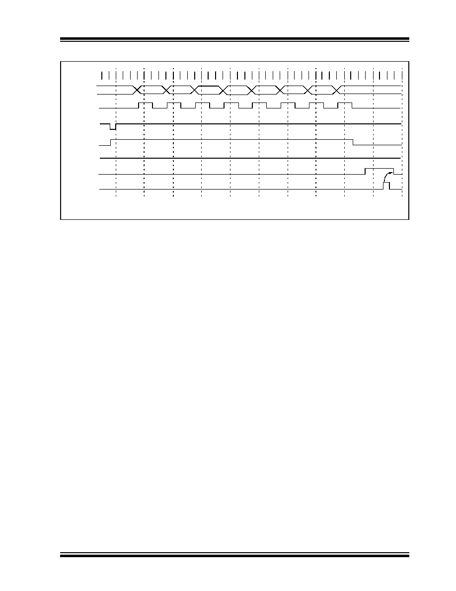
FIGURE 11-11:
SYNCHRONOUS RECEPTION (MASTER MODE, SREN)
11.4
USART Synchronous Slave Mode
Synchronous Slave mode differs from the Master mode
in the fact that the shift clock is supplied externally at
the RC6/TX/CK/SCK/SCL/SEG9 pin (instead of being
supplied internally in Master mode). This allows the
device to transfer or receive data while in Sleep mode.
Slave mode is entered by clearing bit, CSRC
(TXSTA<7>).
11.4.1
USART SYNCHRONOUS SLAVE
TRANSMIT
The operation of the Synchronous Master and Slave
modes is identical, except in the case of the Sleep mode.
If two words are written to the TXREG and then the
SLEEP
instruction is executed, the following will occur:
a)
The first word will immediately transfer to the
TSR register and transmit.
b)
The second word will remain in TXREG register.
c)
Flag bit TXIF will not be set.
d)
When the first word has been shifted out of TSR,
the TXREG register will transfer the second word
to the TSR and flag bit TXIF will now be set.
e)
If enable bit TXIE is set, the interrupt will wake
the chip from Sleep and if the global interrupt is
enabled, the program will branch to the interrupt
vector (0004h).
When setting up a Synchronous Slave Transmission,
follow these steps:
1.
Enable the synchronous slave serial port by set-
ting bits SYNC and SPEN and clearing bit
CSRC.
2.
Clear bits CREN and SREN.
3.
If interrupts are desired, then set enable bit
TXIE.
4.
If 9-bit transmission is desired, then set bit TX9.
5.
Enable the transmission by setting enable bit
TXEN.
6.
If 9-bit transmission is selected, the ninth bit
should be loaded in bit TX9D.
7.
Start transmission by loading data to the TXREG
register.
8.
If using interrupts, ensure that GIE and PEIE
(bits 7 and 6) of the INTCON register are set.
CREN bit
RC7/RX/DT/
RC6/TX/CK/
Write to
bit SREN
SREN bit
RCIF bit
(Interrupt)
Read
RXREG
Note: Timing diagram demonstrates Sync Master mode with bit SREN = 1 and bit BRG = 0.
Q3 Q4Q1Q2 Q3Q4Q1Q2Q3Q4
Q2
Q1Q2Q3Q4Q1Q2Q3Q4 Q1Q2Q3Q4Q1Q2Q3Q4 Q1Q2Q3Q4Q1Q2Q3Q4 Q1Q2Q3Q4
‘0’
bit 0
bit 1
bit 2
bit 3
bit 4
bit 5
bit 6
bit 7
‘0’
Q1Q2Q3Q4
SDI/SDA/SEG8
SCK/SCL/SEG9
发布紧急采购,3分钟左右您将得到回复。
相关PDF资料
ATMEGA169P-16MCU
MCU AVR 16K ISP FLSH 16MHZ 64QFN
AT91SAM7XC256-CU
MCU ARM 256K HS FLASH 100-TFBGA
PIC16LF874A-I/P
IC MCU FLASH 4KX14 EE A/D 40DIP
PIC16F84-10/SO
IC MCU FLASH 1KX14 EE 18SOIC
AT91SAM7XC128-CU
MCU ARM 128K HS FLASH 100-TFBGA
PIC18F2458-I/SO
IC PIC MCU FLASH 12KX16 28SOIC
PIC18F4455-I/P
IC PIC MCU FLASH 12KX16 40DIP
AT91SAM7X256-CU
MCU ARM 256K HS FLASH 100-TFBGA
相关代理商/技术参数
ATMEGA169PV-8MU
功能描述:8位微控制器 -MCU AVR 16K FLASH 512B EE 1K SRAM 5V RoHS:否 制造商:Silicon Labs 核心:8051 处理器系列:C8051F39x 数据总线宽度:8 bit 最大时钟频率:50 MHz 程序存储器大小:16 KB 数据 RAM 大小:1 KB 片上 ADC:Yes 工作电源电压:1.8 V to 3.6 V 工作温度范围:- 40 C to + 105 C 封装 / 箱体:QFN-20 安装风格:SMD/SMT
ATMEGA169PV-8MU SL383
制造商:Atmel Corporation 功能描述:MCU 8BIT ATMEGA RISC 16KB FLASH 2.5V/3.3V/5V 64PIN MLF - Tape and Reel
ATMEGA169PV-8MU
制造商:Atmel Corporation 功能描述:IC 8BIT MCU AVR MEGA 8MHZ 64-QFN
ATMEGA169PV-8MUR
功能描述:8位微控制器 -MCU AVR LCD 16KB FLSH EE 512B 1KB SRAM-8MHZ RoHS:否 制造商:Silicon Labs 核心:8051 处理器系列:C8051F39x 数据总线宽度:8 bit 最大时钟频率:50 MHz 程序存储器大小:16 KB 数据 RAM 大小:1 KB 片上 ADC:Yes 工作电源电压:1.8 V to 3.6 V 工作温度范围:- 40 C to + 105 C 封装 / 箱体:QFN-20 安装风格:SMD/SMT
ATMEGA169V
制造商:ATMEL 制造商全称:ATMEL Corporation 功能描述:8-bit Microcontroller with 16K Bytes In-System Programmable Flash
ATMEGA169V_06
制造商:ATMEL 制造商全称:ATMEL Corporation 功能描述:8-bit Microcontroller with 16K Bytes In-System Programmable Flash
ATMEGA169V-1AC
功能描述:IC MCU 8BIT 16KB FLASH 64TQFP 制造商:microchip technology 系列:AVR? ATmega 包装:托盘 零件状态:停產 核心处理器:AVR 核心尺寸:8-位 速度:1MHz 连接性:SPI,UART/USART,USI 外设:欠压检测/复位,LCD,POR,PWM,WDT I/O 数:53 程序存储容量:16KB(8K x 16) 程序存储器类型:闪存 EEPROM 容量:512 x 8 RAM 容量:1K x 8 电压 - 电源(Vcc/Vdd):1.8 V ~ 5.5 V 数据转换器:A/D 8x10b 振荡器类型:内部 工作温度:0°C ~ 70°C 封装/外壳:64-TQFP 供应商器件封装:64-TQFP(14x14) 基本零件编号:ATmega169 标准包装:160
ATMEGA169V-1AI
制造商:ATMEL 制造商全称:ATMEL Corporation 功能描述:8-bit AVR Microcontroller with 16K Bytes In-System Programmable Flash